
Electronic Component Analysis Services
We provide failure analysis services for semiconductors and electronic components.
We accept analysis requests for products purchased from us as well as from other suppliers.
Both non-destructive and destructive testing are available.
Core Services
| Service | Equipment Used | Inspection Scope |
|---|---|---|
| Authenticity Verification | Microscope / X-ray / Decapsulation Equipment | 1) Visual Inspection 2) X-ray Inspection 3) Surface Removal Inspection (Remarking Check) Comprehensive inspection for counterfeit detection, with detailed report provided |
| Failure Analysis | Microscope / X-ray / Curve Tracer / Decapsulation Equipment | 1) Visual Inspection 2) X-ray Inspection 3) I-V Characteristic Analysis 4) Decapsulation Inspection Optimized analysis based on failure symptoms, with detailed report provided |
- Providing a known-good sample for comparison enables more accurate and reliable analysis.
Individual Inspection Services
| Inspection Type | Equipment Used | Inspection Details |
|---|---|---|
| Visual Inspection | Optical Microscope | Inspection of package, leads, and markings at magnifications from 1× to 1,000× |
| X-ray Inspection | X-ray Imaging System | Inspection of chip size, bonding wire positions, and internal lead frame structure |
| Cross-Sectional FIB Analysis | FIB System | Cross-sectional analysis using a focused ion beam (FIB) system |
| STEM Analysis | Scanning Transmission Electron Microscope (STEM) | High-resolution observation and high-sensitivity analysis of microstructures |
| Cross-Section / Planar Polishing | Polishing Equipment | Cross-sectional observation through mechanical polishing |
| Decapsulation Inspection | Decapsulation System / Microscope | Removal of molding compound using chemicals, followed by inspection of chip surface at 1× to 1,000× magnification |
| Electrical Characteristic Analysis | Curve Tracer | Measurement of I-V characteristics |
Inspection Process
Based on your requirements, we will propose the most suitable plan along with a quotation.
Please send your purchase order to the email address provided in our quotation.
Then ship the test samples and reference samples to the address below:
Address:
5F Tokiwa Building
1-14-16 Kanayama, Naka-ku, Nagoya, Aichi 460-0022, Japan
TEL: +81-52-300-0525
Inspection will be carried out after receiving the test and reference samples.
An inspection report will be issued via email.
The submitted test and reference samples will also be returned.
An invoice will be issued at the end of the delivery month.
Please make payment by the end of the following month.
Equipment
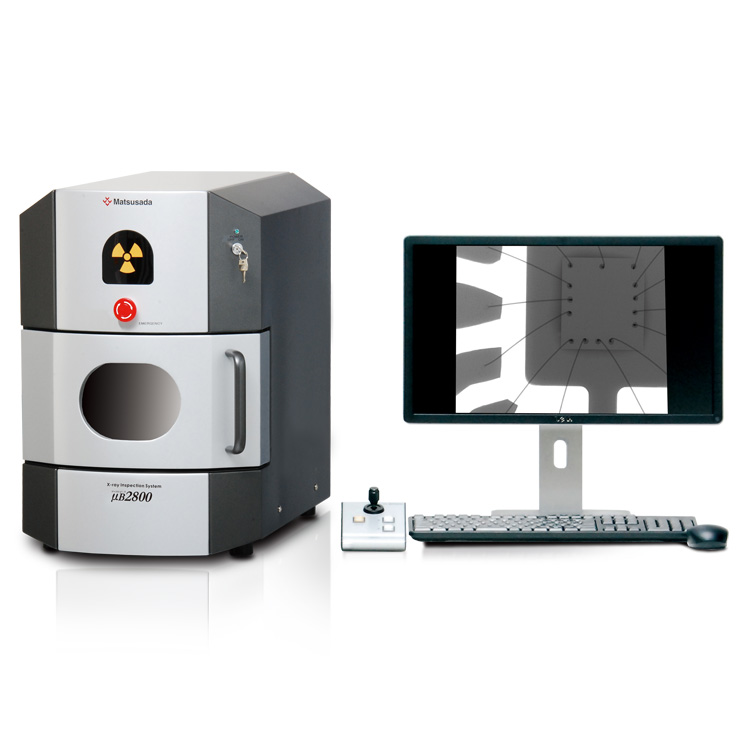
Enables non-destructive observation of internal structures of products, components, and materials, and acquisition of 3D data.
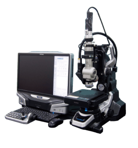
Used for morphological observation and various measurements of samples.
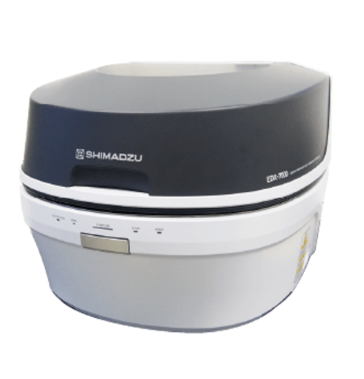
Performs high-sensitivity analysis of trace elements, suitable for material and contaminant analysis.
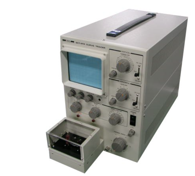
Measures the electrical characteristics of semiconductor devices.
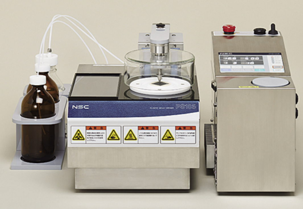
Removes resin to allow internal inspection of IC chips.
CONTACT USFeel free to reach out with any questions or inquiries.
- Screen sharing available for detailed explanations
- Online meetings that feel like face-to-face conversations
- Phone, email, and chat support available